- 您现在的位置:买卖IC网 > Sheet目录342 > MCB11C14 (Keil)BOARD EVAL FOR NXP LPC11C14
�� �
�
�NXP� Semiconductors�
�LPC11C12/C14�
�11.� Application� information�
�11.1� ADC� usage� notes�
�The� following� guidelines� show� how� to� increase� the� performance� of� the� ADC� in� a� noisy�
��?� The� ADC� input� trace� must� be� short� and� as� close� as� possible� to� the� LPC11C12/C14�
�chip.�
�?� The� ADC� input� traces� must� be� shielded� from� fast� switching� digital� signals� and� noisy�
�power� supply� lines.�
�?� Because� the� ADC� and� the� digital� core� share� the� same� power� supply,� the� power� supply�
�line� must� be� adequately� filtered.�
�?� To� improve� the� ADC� performance� in� a� very� noisy� environment,� put� the� device� in� Sleep�
�mode� during� the� ADC� conversion.�
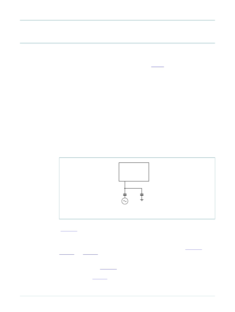
�11.2� XTAL� input�
�The� input� voltage� to� the� on-chip� oscillators� is� limited� to� 1.8� V.� If� the� oscillator� is� driven� by� a�
�clock� in� slave� mode,� it� is� recommended� that� the� input� be� coupled� through� a� capacitor� with�
�C� i� =� 100� pF.� To� limit� the� input� voltage� to� the� specified� range,� choose� an� additional�
�capacitor� to� ground� C� g� which� attenuates� the� input� voltage� by� a� factor� C� i� /(C� i� +� C� g� ).� In� slave�
�mode,� a� minimum� of� 200� mV(RMS)� is� needed.�
�LPC1xxx�
�XTALIN�
�Ci�
�Cg�
�100� pF�
�002aae788�
�Fig� 22.� Slave� mode� operation� of� the� on-chip� oscillator�
�In� slave� mode� the� input� clock� signal� should� be� coupled� by� means� of� a� capacitor� of� 100� pF�
�(� Figure� 22� ),� with� an� amplitude� between� 200� mV(RMS)� and� 1000� mV(RMS).� This�
�corresponds� to� a� square� wave� signal� with� a� signal� swing� of� between� 280� mV� and� 1.4� V.�
�The� XTALOUT� pin� in� this� configuration� can� be� left� unconnected.�
�External� components� and� models� used� in� oscillation� mode� are� shown� in� Figure 23� and� in�
�Table 15� and� Table 16� .� Since� the� feedback� resistance� is� integrated� on� chip,� only� a� crystal�
�and� the� capacitances� C� X1� and� C� X2� need� to� be� connected� externally� in� case� of�
�fundamental� mode� oscillation� (the� fundamental� frequency� is� represented� by� L,� C� L� and�
�R� S� ).� Capacitance� C� P� in� Figure 23� represents� the� parallel� package� capacitance� and� should�
�not� be� larger� than� 7� pF.� Parameters� F� OSC� ,� C� L� ,� R� S� and� C� P� are� supplied� by� the� crystal�
��LPC11C12_C14_0�
�Preliminary� data� sheet�
�All� information� provided� in� this� document� is� subject� to� legal� disclaimers.�
�Rev.� 00.05� —� 23� April� 2010�
�?� NXP� B.V.� 2010.� All� rights� reserved.�
�40� of� 49�
�发布紧急采购,3分钟左右您将得到回复。
相关PDF资料
MCB2470
BOARD EVAL NXP LPC247X SERIES
MCBSTM32EXL
BOARD EVALUATION FOR STM32F103ZE
MCBTMPM330
BOARD EVAL TOSHIBA TMPM330 SER
MCIMX25WPDKJ
KIT DEVELOPMENT WINCE IMX25
MCIMX53-START-R
KIT DEVELOPMENT I.MX53
MCM69C432TQ20
IC CAM 1MB 50MHZ 100LQFP
MCP1401T-E/OT
IC MOSFET DRVR INV 500MA SOT23-5
MCP1403T-E/MF
IC MOSFET DRIVER 4.5A DUAL 8DFN
相关代理商/技术参数
MCB11C14-ED
制造商:ARM Ltd 功能描述:KEIL NXP LPC11C14 EVAL BOARD
MCB11C14U
功能描述:开发板和工具包 - ARM EVAL BOARD FOR NXP LPC11C14 + ULINK2
RoHS:否 制造商:Arduino 产品:Development Boards 工具用于评估:ATSAM3X8EA-AU 核心:ARM Cortex M3 接口类型:DAC, ICSP, JTAG, UART, USB 工作电源电压:3.3 V
MCB11C14UME
功能描述:开发板和工具包 - ARM EVAL BOARD FOR NXP LPC11C14 + ULINK-ME
RoHS:否 制造商:Arduino 产品:Development Boards 工具用于评估:ATSAM3X8EA-AU 核心:ARM Cortex M3 接口类型:DAC, ICSP, JTAG, UART, USB 工作电源电压:3.3 V
MCB11C14UME-ED
制造商:ARM Ltd 功能描述:KEIL NXP LPC11C14 EVAL BOARD
MCB11U10
功能描述:开发板和工具包 - ARM EVAL BOARD FOR NXP LPC11U14
RoHS:否 制造商:Arduino 产品:Development Boards 工具用于评估:ATSAM3X8EA-AU 核心:ARM Cortex M3 接口类型:DAC, ICSP, JTAG, UART, USB 工作电源电压:3.3 V
MCB11U10U
功能描述:开发板和工具包 - ARM EVAL BOARD FOR NXP LPC11U14 + ULINK2
RoHS:否 制造商:Arduino 产品:Development Boards 工具用于评估:ATSAM3X8EA-AU 核心:ARM Cortex M3 接口类型:DAC, ICSP, JTAG, UART, USB 工作电源电压:3.3 V
MCB11U10U-ED
制造商:ARM Ltd 功能描述:KEIL NXP LPC11U10 EVAL BOARD
MCB11U10UME
功能描述:开发板和工具包 - ARM EVAL BOARD FOR NXP LPC11U14 + ULINK-ME
RoHS:否 制造商:Arduino 产品:Development Boards 工具用于评估:ATSAM3X8EA-AU 核心:ARM Cortex M3 接口类型:DAC, ICSP, JTAG, UART, USB 工作电源电压:3.3 V